Corkscrew Photons May Leave Behind a Spontaneous Twist

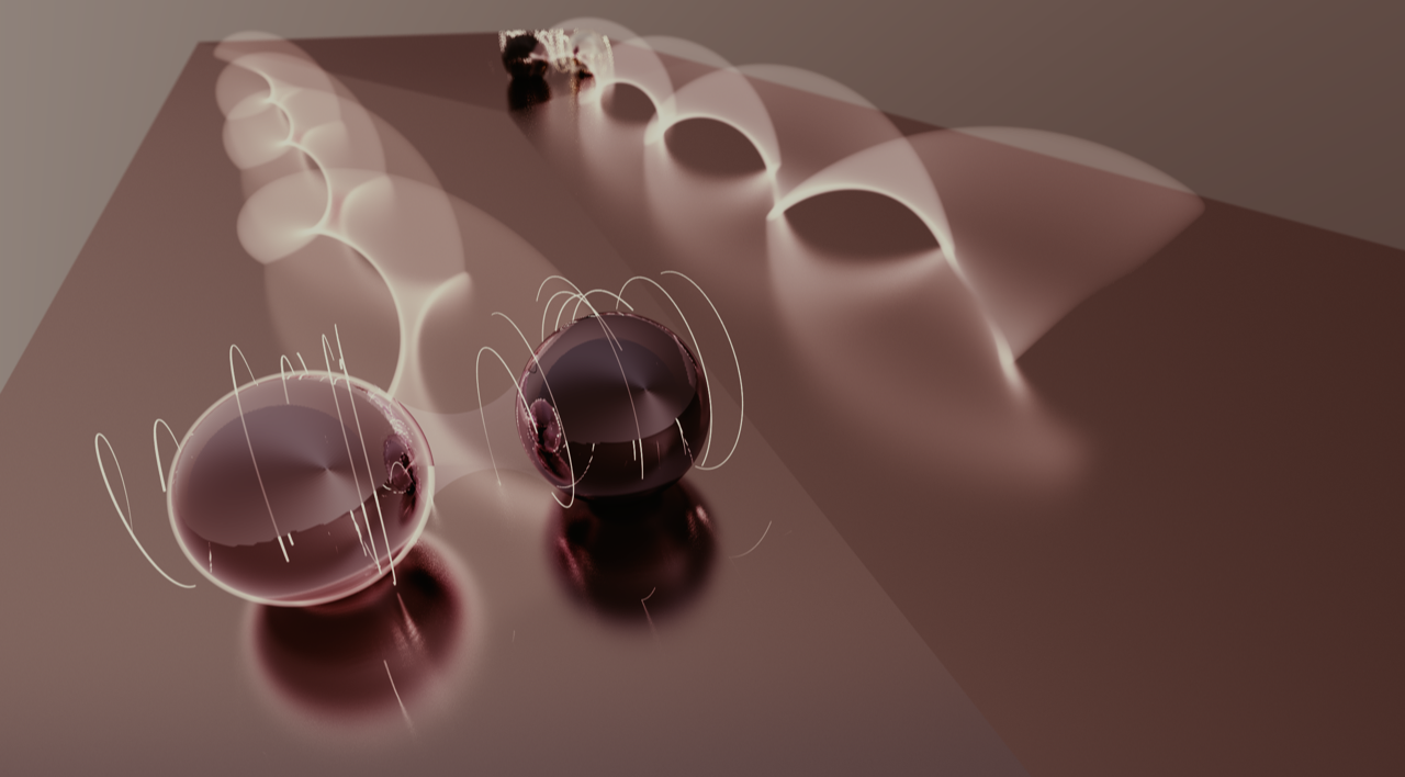
A new prediction argues that some materials might experience a torque when they are hotter than their surroundings. (Credit: E. Edwards/JQI)


Everything radiates. Whether it's a car door, a pair of shoes or the cover of a book, anything hotter than absolute zero (i.e., pretty much everything) is constantly shedding radiation in the form of photons, the quantum particles of light.

A twin process—absorption—is usually also present. As photons carry away energy, passers-by from the environment can be absorbed to replenish it. When absorption and emission occur at the same rate, scientists say that an object is in equilibrium with its environment. This often means that object and environment share the same temperature.

Far away from equilibrium, new behaviors can emerge. In a paper published August 1, 2019 as an Editors’ Suggestion in the journal Physical Review Letters, scientists at JQI and Michigan State University suggest that certain materials may experience a spontaneous twisting force if they are hotter than their surroundings.

"The fact that a material might feel a torque due to a temperature difference with the environment is very unusual," says lead author Mohammad Maghrebi, a former JQI postdoctoral researcher who is now an assistant professor at Michigan State University.

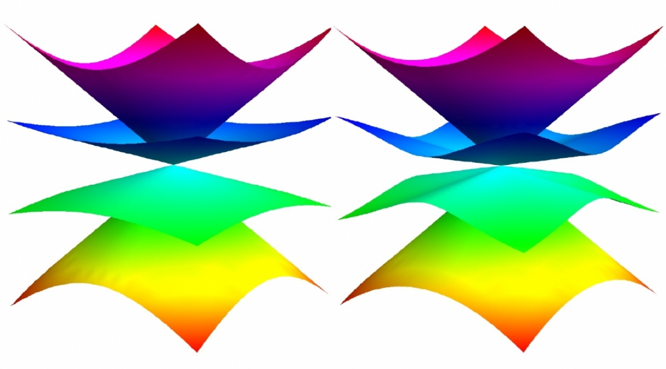
The effect, which hasn't yet been observed in an experiment, is predicted to arise in a thin ribbon of a material called a topological insulator (TI)—something that allows electrical current to flow on its surface but not through its innards.

In this case, the researchers made two additional assumptions about the TI. One is that it is hotter than its environment. And another is that the TI has some magnetic impurities that affect the behavior of electrons on its surface.

These magnetic impurities interact with a quantum property of the electrons called spin. Spin is part of the basic character of an electron, much like electric charge, and it describes the particle’s intrinsic angular momentum—the tendency of an object to continue rotating. Photons, too, can carry angular momentum.

Although electrons don’t physically rotate, they can still gain and lose angular momentum, albeit only in discrete chunks. Each electron has two spin values—up and down—and the magnetic impurities ensure that one value sits at a higher energy than the other. In the presence of these impurities, electrons can flip their spin from up to down and vice versa by emitting or absorbing a photon that carries the right amount of energy and angular momentum.

Maghrebi and two colleagues, JQI Fellows Jay Deep Sau and Alexey Gorshkov, showed that radiation emanating from this kind of TI carries angular momentum skewed in one rotational direction, like a corkscrew that twists clockwise. The material gets left with a deficit of angular momentum, causing it to feel a torque in the opposite direction (in this example, counterclockwise).

The authors say that TIs are ideal for spotting this effect because they play host to the right kind of interaction between electrons and light. TIs already link electron spin with the momentum of their motion, and it's through this motion that electrons in the material ordinarily absorb and emit light.

If an electron on the surface of this particular kind of TI starts with its spin pointing up, it can shed energy and angular momentum by changing its spin from up to down and emitting a photon. Since the TI is hotter than its environment, electrons will flip from up to down more often than the reverse. That’s because the environment has a lower temperature and lacks the energy to replace the radiation coming from the TI. The result of this imbalance is a torque on the thin TI sample, driven by the random emission of radiation.

Future experiments might observe the effect in one of two ways, the authors say. The most likely method is indirect, requiring experimenters to heat up a TI by running a current through it and collecting the emitted light. By measuring the average angular momentum of the radiation, an experiment might detect the asymmetry and confirm one consequence of the new prediction.

A more direct—and likely more difficult—observation would involve actually measuring the torque on the thin film by looking for tiny rotations. Maghrebi says that he's brought up the idea to several experimentalists. "They were not horrified by having to measure something like a torque, but, at the same time, I think it really depends on the setup," he says. "It certainly didn't sound like it was impossible."

Story by Chris Cesare: https://jqi.umd.edu/news/corkscrew-photons-may-leave-behind-spontaneous-twist

Research Contact
Alexey Gorshkov
This email address is being protected from spambots. You need JavaScript enabled to view it.
Media Contact
Chris Cesare
This email address is being protected from spambots. You need JavaScript enabled to view it.
 

Currie to Send Next Gen Retroreflectors to Moon

In 1969, University of Maryland physicist Doug Currie helped design three still-in-use lunar instruments placed on the moon by Apollo 11, 14 and 15. Fifty years later, Currie is lead scientist for a just-approved NASA project to place next-generation versions of these instruments on the Moon.

Known as lunar retroreflectors, the instruments reflect laser pulses sent from Earth back to their exact origin point, allowing precise measurements of the Earth-moon distance; providing data to better understand aspects of the moon’s interior, including its liquid core; testing questions of fundamental physics, and allowing better mapping and navigation of the lunar surface.  

According to Currie, a senior research scientist and professor emeritus at the University of Maryland, the new UMD-led project can lead to improvements in all of these research areas: (1) because of the hundred fold improvement in the accuracy of individual ranges using the new retroreflectors and (2) by the increased accuracy produced by a larger number of reflectors with a wider lunar area covered by the network.  Currently, there are five retroreflectors on the moon: the three placed by Apollo missions and two French-designed instruments placed by Soviet lunar missions. The Currie-led proposal would add three Next Generation Retroreflectors for a total of eight lunar retroreflector arrays. 

“Our Next Generation Lunar Retroreflector is a 21st Century version of the instruments currently on the Moon. Each placement of a Next Generation lunar laser ranging array will greatly enhance the scientific and navigational capabilities of retroreflector network,” said Currie. “These additions improve the mapping and navigation capabilities important for NASA’s plans to return to the Moon and by 2028 establish a sustained human presence.” 

“And these also will significantly boost scientists’ ability to use the network to conduct important science, such as new tests of general relativity and other theories of gravity. Such studies may help us understand the nature of mysterious dark matter, which appears to constitute almost 27 percent of the Universe,” he said. 

According to a NASA release, the Next Generation Lunar Retroreflectors (NGLR) is one of 12 new science and technology payloads selected by the agency to help humans study the Moon and explore more of its surface as part of the NASA’s Artemis lunar program. The agency says the retroreflector and the other 11 investigations and demonstrations “will help the agency to send astronauts to the Moon by 2024 as a way to prepare to send humans to Mars for the first time.”

The selected investigations will go to the Moon on future flights through NASA's Commercial Lunar Payload Services (CLPS) project. According to the agency, the CLPS project allows rapid acquisition of lunar delivery services for payloads like these that advance capabilities for science, exploration, or commercial development of the Moon. 

NASA has selected the first three commercial Moon landing service providers that will deliver science and technology payloads to the lunar surface. According to Currie, the Next Generation Retroreflectors are not currently scheduled by NASA to be among the payloads carried on those three commercial Moon landings. “However, we believe because of the low size and weight of these retroreflectors, each mission could safely add one to their planned payloads for each of these commercial delivery missions,” he said. 

"The selected lunar payloads represent cutting-edge innovations, and will take advantage of early flights through our commercial services project,” said Thomas Zurbuchen, associate administrator of the agency's Science Mission Directorate in Washington. "Each demonstrates either a new science instrument or a technological innovation that supports scientific and human exploration objectives, and many have broader applications for Mars and beyond.”

The NGLR team consists of Currie as Principal Investigator and Simone Dell’Agnello of the Istituto Nazionale di Fisica Nucleare, Laboratori Nazionali di Frascati, Italy, as Co-I/Co-PI. Co-Investigators are Christopher Davis of the UMD Electrical and Computer Engineering Department; Giovanni Delle Monache, also of the Istituto Nazionale di Fisica Nucleare; James Williams of the Jet Propulsion Laboratory; and John Rzasa and Dennis Wellnitz of the UMD Department of Astronomy. Assistant Research Scientist Chensheng Wu, a member of Professor Chris Davis’ Maryland Optical Group, has also done crucial work on the design of the Next Generation Lunar Retroreflectors.

(Currie was interviewed by ABC News about the 50th anniversary of Apollo 11.)

Links for more information:

What Neil & Buzz Left on the Moon | NASA Science Mission Directorate

NASA Selects 12 New Lunar Science, Technology Investigations 

currie

Pictured (L-R) in 1969 are University of Maryland (UMD) physicist Doug Currie, University of Texas (UT) McDonald Observatory Director Harlan J. Smith, NASA Scientist-Astronaut Philip Chapman, UMD Professor of Physics Carroll Alley and NASA Scientist-Astronaut Don L. Lind discussing use of the McDonald Lunar Laser Ranging Observatory (MLLRO) to send short laser pulses to the first Lunar Laser Ranging (LLR) Retroreflector left on the lunar surface by the Apollo 11 Astronauts. The MLLRO program was developed and initially operated by Professor Currie (then associate professor) with the support of the Godard Space Craft Center and the University of Texas. UMD’s Professor Alley was the Principle Investigator of the project to place LLRs on the moon to address lunar physics, gravitation, General Relativity and Earth physics.  The LLR Retroreflectors were designed and developed by a team that in addition to UMD physicists Alley and Currie, included scientists from universities and federal institutions that included Princeton University, NASA Goddard Space Craft Center, the National Bureau of Standards, Wesleyan University and the University of California. NASA’s Scientist-Astronaut program trained Ph.D. scientists & engineers as astronauts. Image courtesy Doug Currie.

Original story: https://umdrightnow.umd.edu/news/umd-physicist-apollo-experiment-gets-chance-send-next-gen-version-moon

Contact: This email address is being protected from spambots. You need JavaScript enabled to view it. 301-405-4679

Perfect Quantum Portal Emerges at Exotic Interface

klein tunneling gallery lrIn Klein tunneling, an electron can transit perfectly through a barrier. In a new experiment, researchers observed the Klein tunneling of electrons into a special kind of superconductor. (Credit: E. Edwards/JQI)

A junction between an ordinary metal and a special kind of superconductor has provided a robust platform to observe Klein tunneling.

Researchers at the University of Maryland have captured the most direct evidence to date of a quantum quirk that allows particles to tunnel through a barrier like it’s not even there. The result, featured on the cover of the June 20, 2019 issue of the journal Nature, may enable engineers to design more uniform components for future quantum computers, quantum sensors and other devices.

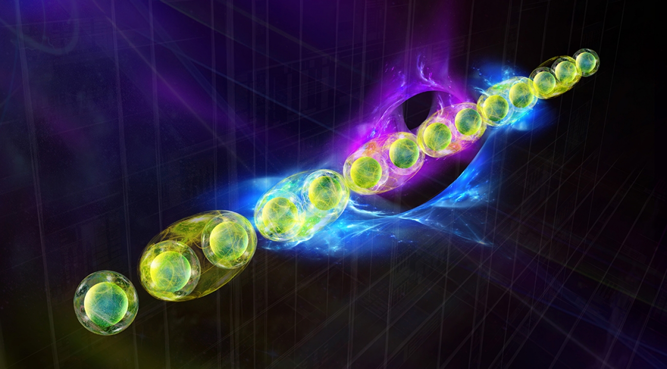
The new experiment is an observation of Klein tunneling, a special case of a more ordinary quantum phenomenon. In the quantum world, tunneling allows particles like electrons to pass through a barrier even if they don’t have enough energy to actually climb over it. A taller barrier usually makes this harder and lets fewer particles through.

Klein tunneling occurs when the barrier becomes completely transparent, opening up a portal that particles can traverse regardless of the barrier’s height. Scientists and engineers from UMD’s Center for Nanophysics and Advanced Materials (CNAM), the Joint Quantum Institute (JQI) and the Condensed Matter Theory Center (CMTC), with appointments in UMD’s Department of Materials Science and Engineering and Department of Physics, have made the most compelling measurements yet of the effect.

“Klein tunneling was originally a relativistic effect, first predicted almost a hundred years ago,” says Ichiro Takeuchi, a professor of materials science and engineering (MSE) at UMD and the senior author of the new study. “Until recently, though, you could not observe it.”

It was nearly impossible to collect evidence for Klein tunneling where it was first predicted—the world of high-energy quantum particles moving close to the speed of light. But in the past several decades, scientists have discovered that some of the rules governing fast-moving quantum particles also apply to the comparatively sluggish particles traveling near the surface of some unusual materials.

One such material—which researchers used in the new study—is samarium hexaboride (SmB6), a substance that becomes a topological insulator at low temperatures. In a normal insulator like wood, rubber or air, electrons are trapped, unable to move even when voltage is applied. Thus, unlike their free-roaming comrades in a metal wire, electrons in an insulator can’t conduct a current.

Topological insulators such as SmB6 behave like hybrid materials. At low enough temperatures, the interior of SmB6 is an insulator, but the surface is metallic and allows electrons some freedom to move around. Additionally, the direction that the electrons move becomes locked to an intrinsic quantum property called spin that can be oriented up or down. Electrons moving to the right will always have their spin pointing up, for example, and electrons moving left will have their spin pointing down.

The metallic surface of SmB6 would not have been enough to spot Klein tunneling, though. It turned out that Takeuchi and colleagues needed to transform the surface of SmB6 into a superconductor—a material that can conduct electrical current without any resistance.

To turn SmB6 into a superconductor, they put a thin film of it atop a layer of yttrium hexaboride (YB6). When the whole assembly was cooled to just a few degrees above absolute zero, the YB6 became a superconductor and, due to its proximity, the metallic surface of SmB6 became a superconductor, too.

It was a “piece of serendipity” that SmB6 and its yttrium-swapped relative shared the same crystal structure, says Johnpierre Paglione, a professor of physics at UMD, the director of CNAM and a co-author of the research paper. “However, the multidisciplinary team we have was one of the keys to this success. Having experts on topological physics, thin-film synthesis, spectroscopy and theoretical understanding really got us to this point,” Paglione adds.

The combination proved the right mix to observe Klein tunneling. By bringing a tiny metal tip into contact with the top of the SmB6, the team measured the transport of electrons from the tip into the superconductor. They observed a perfectly doubled conductance—a measure of how the current through a material changes as the voltage across it is varied.

“When we first observed the doubling, I didn’t believe it,” Takeuchi says. “After all, it is an unusual observation, so I asked my postdoc Seunghun Lee and research scientist Xiaohang Zhang to go back and do the experiment again.”

When Takeuchi and his experimental colleagues convinced themselves that the measurements were accurate, they didn’t initially understand the source of the doubled conductance. So they started searching for an explanation. UMD’s Victor Galitski, a JQI Fellow, a professor of physics and a member of CMTC, suggested that Klein tunneling might be involved.

“At first, it was just a hunch,” Galitski says. “But over time we grew more convinced that the Klein scenario may actually be the underlying cause of the observations.”

Valentin Stanev, an associate research scientist in MSE and a research scientist at JQI, took Galitski’s hunch and worked out a careful theory of how Klein tunneling could emerge in the SmB6 system—ultimately making predictions that matched the experimental data well.

The theory suggested that Klein tunneling manifests itself in this system as a perfect form of Andreev reflection, an effect present at every boundary between a metal and a superconductor. Andreev reflection can occur whenever an electron from the metal hops onto a superconductor. Inside the superconductor, electrons are forced to live in pairs, so when an electron hops on, it picks up a buddy.

In order to balance the electric charge before and after the hop, a particle with the opposite charge—which scientists call a hole—must reflect back into the metal. This is the hallmark of Andreev reflection: an electron goes in, a hole comes back out. And since a hole moving in one direction carries the same current as an electron moving in the opposite direction, this whole process doubles the overall conductance—the signature of Klein tunneling through a junction of a metal and a topological superconductor.

In conventional junctions between a metal and a superconductor, there are always some electrons that don’t make the hop. They scatter off the boundary, reducing the amount of Andreev reflection and preventing an exact doubling of the conductance.

But because the electrons in the surface of SmB6 have their direction of motion tied to their spin, electrons near the boundary can’t bounce back—meaning that they will always transit straight into the superconductor.

“Klein tunneling had been seen in graphene as well,” Takeuchi says. “But here, because it’s a superconductor, I would say the effect is more spectacular. You get this exact doubling and a complete cancellation of the scattering, and there is no analog of that in the graphene experiment.”

Junctions between superconductors and other materials are ingredients in some proposed quantum computer architectures, as well as in precision sensing devices. The bane of these components has always been that each junction is slightly different, Takeuchi says, requiring endless tuning and calibration to reach the best performance. But with Klein tunneling in SmB6, researchers might finally have an antidote to that irregularity.

“In electronics, device-to-device spread is the number one enemy,” Takeuchi says. “Here is a phenomenon that gets rid of the variability.”

Story by Chris Cesare

In addition to Takeuchi, Paglione, Lee, Zhang, Galitski and Stanev, co-authors of the research paper include Drew Stasak, a former research assistant in MSE; Jack Flowers, a former graduate student in MSE; Joshua S. Higgins, a research scientist in CNAM and the Department of Physics; Sheng Dai, a research fellow in the department of chemical engineering and materials science at the University of California, Irvine (UCI); Thomas Blum, a graduate student in physics and astronomy at UCI; Xiaoqing Pan, a professor of chemical engineering and materials science and of physics and astronomy at UCI; Victor M. Yakovenko, a JQI Fellow, professor of physics at UMD and a member of CMTC; and Richard L. Greene, a professor of physics at UMD and a member of CNAM.

Ring Resonators Corner Light

Researchers at the Joint Quantum Institute (JQI) have created the first silicon chip that can reliably constrain light to its four corners. The effect, which arises from interfering optical pathways, isn't altered by small defects during fabrication and could eventually enable the creation of robust sources of quantum light.

That robustness is due to topological physics, which describes the properties of materials that are insensitive to small changes in geometry. The cornering of light, which was reported June 17 in Nature Photonics, is a realization of a new topological effect, first predicted in 2017.

hafezi quadrupole2 copyA new, grooved silicon chip keeps light in the corners using the physics of quadrupoles and topology. (Credit: E. Edwards/JQI)

In particular, the new work is a demonstration of quadrupole topological physics. A quadrupole is an arrangement of four poles—sinks and sources of force fields such as electrical charges or the poles of a magnet. You can visualize an electric quadrupole by imagining charges on each corner of a square that alternate positive-negative-positive-negative as you go along the perimeter.

The fact that the cornering arises from quadrupole physics instead of the physics of dipoles—that is, arrangements of just two poles—means it a higher-order topological effect.

Although the cornering effect has been observed in acoustic and microwave systems before, the new work is the first time it’s been observed in an optical system, says Associate Professor and JQI Fellow Mohammad Hafezi, the paper’s senior author. "We have been developing integrated silicon photonic systems to realize ideas derived from topology in a physical system," Hafezi says. "The fact that we use components compatible with current technology means that, if these systems are robust, they could possibly be translated into immediate applications."

In the new work, laser light is injected into a grid of resonators—grooved loops in the silicon that confine the light to rings. By placing the resonators at carefully measured distances, it's possible to adjust the interaction between neighboring resonators and alter the path that light takes through the grid.

The cumulative effect is that the light in the middle of the chip interferes with itself, causing most of the light injected into the chip to spend its time at the four corners.

Light doesn’t have an electric charge, but the presence or absence of light in a given resonator provides a kind of polar behavior. In this way, the pattern of resonators on the chip corresponds to a collection of interacting quadrupoles—precisely the conditions required by the first prediction of higher-order topological states of matter.

To test their fabricated pattern, Hafezi and his colleagues injected light into each corner of the chip and then captured an image of the chip with a microscope. In the collected light, they saw four bright peaks, one at each corner of the chip.

To show that the cornered light was trapped by topology, and not merely a result of where they injected the lasers, they tested a chip with the bottom two rows of resonators shifted. This changed their interactions with the resonators above, and, at least theoretically, changed where the bright spots should appear. They again injected the light at the corners, and this time—just as theory predicted—the lower two bright spots showed up above the rows of shifted resonators and not at the physical corners.

Despite the protection from small changes in resonator placement offered by topology, a second, more destructive fabrication defect remains in these chips. Since each resonator isn't exactly the same, the four points of light at the corners all shine with slightly different frequencies. This means that, for the moment, the chip may be no better than a single resonator if used as a source of photons—the quantum particles of light that many hope to harness as carriers of quantum information in future devices and networks.

"If you have many sources that are forced by topology to spit out identical photons, then you could interfere them, and that would be a game-changer," says Sunil Mittal, the lead author of the paper and a postdoctoral researcher at JQI. "I hope this work actually excites theorists to think about maybe looking for models that are insensitive to this lingering disorder in resonator frequencies."

Story by Chris Cesare

Hafezi and Mittal also have affiliations in the Department of Electrical and Computer Engineering, as well as the Institue for Research in Electronics and Applied Physics. Hafezi is also an associate professor in the Department of Physics.

High-resolution Imaging Technique Maps out an Atomic Wave Function

Overlapping Laser Beams Offer a New Way to Extract A Quantum System's Essential Information

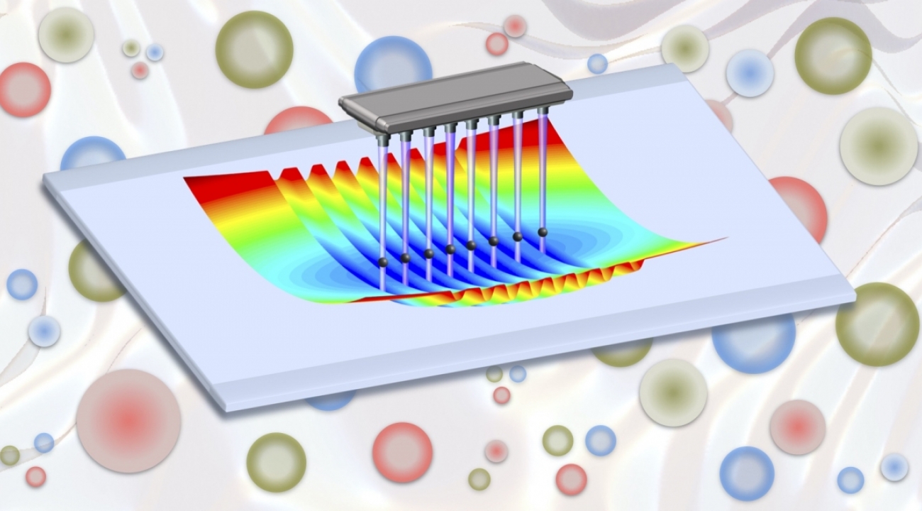
19pml013 wavefunction porto rolston 2mbThe team has used laser light to construct an image of an atomic wave function (shown in purple). The graphic is an artistic depiction of this process, showing a microscope objective trained on atoms (spheres) suspended in an optical lattice (tall white waves). The team's technique reveals information about an atomic wave function in unprecedented detail.

From NIST News

JQI researchers have demonstrated a new way to obtain the essential details that describe an isolated quantum system, such as a gas of atoms, through direct observation. The new method gives information about the likelihood of finding atoms at specific locations in the system with unprecedented spatial resolution. With this technique, scientists can obtain details on a scale of tens of nanometers—smaller than the width of a virus.

The new experiments use an optical lattice—a web of laser light that suspends thousands of individual atoms—to determine the probability that an atom might be at any given location. Because each individual atom in the lattice behaves like all the others, a measurement on the entire group of atoms reveals the likelihood of an individual atom to be in a particular point in space.  

Published in the journal Physical Review X, the technique (similar work was published simultaneously by a group at the University of Chicago) can yield the likelihood of the atoms’ locations at well below the wavelength of the light used to illuminate the atoms—50 times better than the limit of what optical microscopy can normally resolve. 

“It’s a demonstration of our ability to observe quantum mechanics,” says JQI Fellow and NIST physicist Trey Porto, one of the researchers behind the effort. “It hasn’t been done with atoms with anywhere near this precision.”

To understand a quantum system, physicists talk frequently about its “wave function.” It is not just an important detail; it’s the whole story. It contains all the information you need to describe the system.   

“It’s the description of the system,” says JQI Fellow and UMD physics professor Steve Rolston, another of the paper’s authors. “If you have the wave function information, you can calculate everything else about it—such as the object’s magnetism, its conductivity and its likelihood to emit or absorb light.”

While the wave function is a mathematical expression and not a physical object, the team’s method can reveal the behavior that the wave function describes: the probabilities that a quantum system will behave in one way versus another. In the world of quantum mechanics, probability is everything. 

Among the many strange principles of quantum mechanics is the idea that before we measure their positions, objects may not have a pinpointable location. The electrons surrounding the nucleus of an atom, for example, do not travel in regular planetlike orbits, contrary to the image some of us were taught in school. Instead, they act like rippling waves, so that an electron itself cannot be said to have a definite location. Rather, the electrons reside within fuzzy regions of space.

All objects can have this wavelike behavior, but for anything large enough for unaided eyes to see, the effect is imperceptible and the rules of classical physics are in force—we don’t notice buildings, buckets or breadcrumbs spreading out like waves. But isolate a tiny object such as an atom, and the situation is different because the atom exists in a size realm where the effects of quantum mechanics reign supreme. It’s not possible to say with certainty where it’s located, only that it will be found somewhere. The wave function provides the set of probabilities that the atom will be found in any given place. 

Quantum mechanics is well-enough understood—by physicists, anyway—that for a simple-enough system, experts can calculate the wave function from first principles without needing to observe it. Many interesting systems are complicated, though.

“There are quantum systems that can’t be calculated because they are too difficult,” Rolston says—such as molecules made of several large atoms. “This approach could help us understand those situations.”

As the wave function describes only a set of probabilities, how can physicists get a complete picture of its effects in short order? The team’s approach involves measuring a large number of identical quantum systems at the same time and combining the results into one overall picture. It’s sort of like rolling 100,000 pairs of dice at the same time—each roll gives a single result, and contributes a single point on the probability curve showing the values of all the dice. 

What the team observed were the positions of the roughly 100,000 atoms of ytterbium the optical lattice suspends in its lasers. The ytterbium atoms are isolated from their neighbors and restricted to moving back and forth along a one-dimensional line segment. To get a high-resolution picture, the team found a way to observe narrow slices of these line segments, and how often each atom showed up in its respective slice. After observing one region, the team measured another, until it had the whole picture.

Rolston says that while he hasn’t yet thought of a “killer app” that would take advantage of the technique, the mere fact that the team has directly imaged something central to quantum research fascinates him. 

“It’s not totally obvious where it will be used, but it’s a new technique that offers new opportunities,” he said. “We’ve been using an optical lattice to capture atoms for years, and now it’s become a new kind of measurement tool.” 

The original story was written by C. Boutin/NIST. Minor modifications were made for posting to this website.